上海埃飞科技
Worldwide Technology(S. H)上海埃飞科技
Worldwide Technology(S. H)产品展示
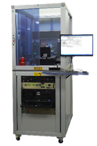

Photoacoustic non-destructive film thickness meter
The photoacoustic non-destructive film thickness meter provides a solution to many problems related to these evolutions. Defect detection is now essential in many industries to avoid problems in the production process and improve quality.
With the rise of the electronics and nanoscience era, the miniaturization of electronic components has become an important factor in their almost exponential performance. Thinning the technical layers and coatings to the nanometer level can make progress in various fields. Complicated manufacturing processes are driving the control to become more and more accurate.
The photoacoustic non-destructive film thickness meter provides a solution to many problems related to these evolutions. Defect detection is now essential in many industries to avoid problems in the production process and improve quality.
We designed a photoacoustic non-destructive measurement system using patented photoacoustic technology. The technology originated from the technology transfer of French CNRS and the University of Bordeaux. It relies on the interaction between lasers, materials and sound waves to penetrate into the core of matter.
Our non-destructive and non-contact technology converts light into sound waves with audio frequencies exceeding 100 GHz. The purpose is to characterize the coating, such as the thickness and adhesion of different types of materials. It is especially suitable for measuring thin layers from a few nanometers to a few microns, whether it is opaque (metals, metal oxides and ceramics), or translucent and transparent. This 100% optical technology is not affected by the shape of the sample.
Features
• Non-destructive and non-contact technology
• Characterization of the film: thickness, adhesion, thermal properties
• Fast and repeatable measurement
• Ultra-precision measurement
• Many materials are available
• The film thickness that can be detected is from 2 nanometers to 20 microns
• Scanning method: single point, XY scan, surface acoustic wave
• Types of test samples: opaque, translucent, and transparent can be tested.
• Both flat and curved samples are available
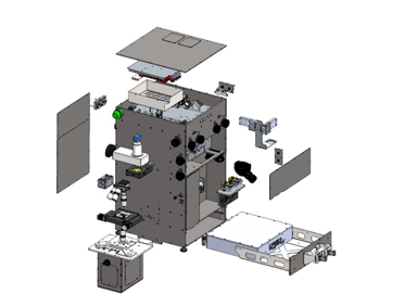
System Components:
The photoacoustic lossless film thickness meter uses two synchronized ultrafast lasers. Laser pulses of different wavelengths of approximately 100 femtoseconds are generated. Use these pulses for non-destructive and non-contact measurements. These are concentrated on the surface of the sample under study.
Materials that can be used
The wide range of materials and their use in many applications make this material aspect indispensable. Since the product came out, our technology has proven its ability to measure many metal materials. It is also suitable for ceramics and metal oxides, and is not affected by shape factors.
The following are the materials that can be used.
Non-destructive testing (NDT) specific application cases in the semiconductor industry
The semiconductor industry provides basic components for most electronic devices encountered around us. Its manufacturing requires multiple thin film depositions on silicon wafers.
problem?
In any process, the deposition of opaque films, whether single-layer or multi-layer, requires quality control. Whether it is inspection or metrology, thickness measurement and interface characterization are key issues to ensure its quality.
Our solution?
-High speed control.
-Non-destructive and non-contact measurement.
-Single-layer and multi-layer thickness measurement.
Display industry
Today, different technologies compete to dominate the production of displays, and displays are ubiquitous in our daily use. In fact, due to the future UHD-8K standard and the emerging flexible display manufacturing process, there are technical limitations in this expanding industry.
problem?
A pixel is still a pile of thin layers of organic ink, silver, ITO... In this regard, the problem of controlling the thickness of the thin layer still exists. These problems may cause quality defects in the final product.
Our solution?
-Unique inspection of such layers.
-Possibility to extract thickness.
-Non-destructive and non-contact thickness measurement.
Thin layer deposition
Whether in the aerospace industry or medical device manufacturing, technical coatings can be used to enhance certain functions in high value-added components. The thickness of these coatings then becomes a key factor in ensuring the target performance.
problem?
Whether it is legal or technical limitations, sampling methods for destructive testing often provide incomplete answers. In addition, it is difficult to control 3D works due to factors such as shape factors and curvature.
Our solution
-Non-destructive and non-contact testing
-Quickly test thickness data
-Online production control is now possible
因用于机器人各方面应用且与大多数机器人类型兼容,AutoCal系统可以检测出机器人自身构造和工具中心点(TCP)的 突然改变或偏离,并且该系统无需人为干涉就自动地更正这些误差。
AutoCal系统-Dynalog的先进水平校准技术,Dynalog是机器人单元标定技术的世界领导者。它的主流产品DynaCal 系统,被应用于离线的机器人单元校准,并作为最精确的和技术先进的机器人校准程序为许多机器人制造商和终端使用者所接受。AutoCal 系统将已证实的DynaCal校准技术结合到一个在线的全自动系统中,该系统专为程序控制和复原而设计的,价格低廉。
AutoCal系统提供在线的机器人校准方案,旨在快速和自动地保证机械设备的工作性能。因用于机器人各方面应用且与大多数机器人类型兼容,AutoCal系统可以检测出机器人自身构造和工具中心点(TCP)的 突然改变或偏离,并且该系统无需人为干涉就自动地更正这些误差。这意味着不用猜测哪里会出错,不用浪费宝贵时间在机器人程序重复校准上,产品品质无任何损失。
AutoCal系统-Dynalog的先进水平校准技术,Dynalog是机器人单元标定技术的世界领导者。它的主流产品DynaCal 系统,被应用于离线的机器人单元校准,并作为最精确的和技术先进的机器人校准程序为许多机器人制造商和终端使用者所接受。AutoCal 系统将已证实的DynaCal校准技术结合到一个在线的全自动系统中,该系统专为程序控制和复原而设计的,价格低廉。